Characteristics and parameters of a bipolar transistor - theoretical introduction
Main topics:
- the principle of operation of the bipolar transistor,
- characteristic of a bipolar transistor,
- transistor transfer characteristics,
- equivalent diagram of the transistor,
- operating ranges of the transistor and limitations of its operating conditions.
The principle of operation of the bipolar transistor
The aim of this lesson is to familiarize yourself with the properties of bipolar transistors as controlled elements, a description of their operation as current sources, and methods of analyzing circuits containing such elements.
A bipolar transistor consists of two p-n junctions arranged in such a way that a common region, e.g. p-type, is created between two n-type regions. Such a transistor is said to be of the npn type. If the areas are arranged in reverse order, then the transistor is pnp type. The figure below shows both types of bipolar transistors together with external sources biasing both junctions.
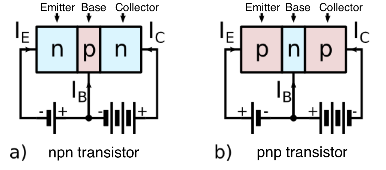
Figure 1
The individual areas with their leads are called: emitter, base, collector. In the normal operating mode of the transistor, the junctions are polarized as follows: emitter junction (base-emitter) - in the forward direction, collector junction (collector-base) in the reverse direction.
The operation of the npn transistor in Figure (a) can be simplified as follows. By biasing the emitter junction in the forward direction, electrons are injected from the emitter into the base region, and holes from the base region into the emitter. Therefore, the emitter current has two components: electron and hole. But only the first one has a significant share in the emitter current, due to the fact that the density of electrons injected from the emitter into the base is much higher than the density of holes injected from the base into the emitter. This is achieved by doping the emitter much more heavily than the base in the manufacturing process, resulting in a much higher dopant concentration in the emitter than in the base.
Once injected into the base, electrons move through the base by diffusion, with a small fraction recombining with holes in the base. The phenomenon of recombination is a driving factor for this diffusion and therefore essential. Due to recombination, only part of the emitter current reaches the collector, and there is also a base current that compensates for the loss of holes in the base area. To ensure the best transfer of current from the emitter to the collector, the base area is made as narrow as possible, because then the electrons diffusing shorter through the base have less chance of recombining with holes. The recombination current is an important component of the base current and control of the recombination current allows control of the collector current.
When the electrons reach the collector junction, they are sucked into the collector area, due to the action of the electric field in this junction, polarized in the reverse direction (in the figure (a), electrons are attracted towards the collector with a positive potential relative to the base). If the voltage polarizing the collector junction is high, electron-hole pairs are formed in the collector area as a result of the avalanche multiplication of the current carriers. The effect of this is that the collector current can be greater than the current of electrons sucked from the base to the collector.
The combined effect of these factors is that the collector current depends on the emitter current (approximately proportionally) and is almost independent of the collector-base voltage. This allows us to conclude that from the side of the output terminals the bipolar transistor behaves like a current source, but not independent, just controlled by the emitter current. There is an emitter junction in the control circuit and therefore the bipolar transistor behaves like a conductive diode from the input terminals side. If the common electrode for the input circuit and the output circuit is the base, then the simplest equivalent circuit of the npn bipolar transistor has the form of a four-circuit as shown in the figure below:
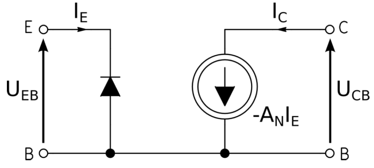
Figure 2
The ratio of the collector current to the emitter current is called the current gain of the transistor in a common-base circuit. Its value (slightly less than one under normal conditions) depends on whether it is given for large (sign: \(A\)) or for small signals (mark \(\alpha\)); sometimes they are taken to be equal to the first approximation: \(A \approx \alpha \). For the DC components of the emitter and collector currents, the collector current \(I_C\) can be represented as \(–AI_E\) , the minus sign taking into account that, according to the general convention, all currents were directed to the appropriate terminals from outside the transistor, which does not cover everywhere with the directions of real currents (in Fig. 1a \(I_E < 0\), and in Fig. 1b \(I_B <0\) and \(I_C <0\)).
Commonly used transistor symbols are shown in the figure below; they use the arrows at the emitter tip to indicate the true direction of the emitter current under emitter junction conduction conditions, and thereafter distinguish the npn transistor from the pnp transistors in the diagrams.
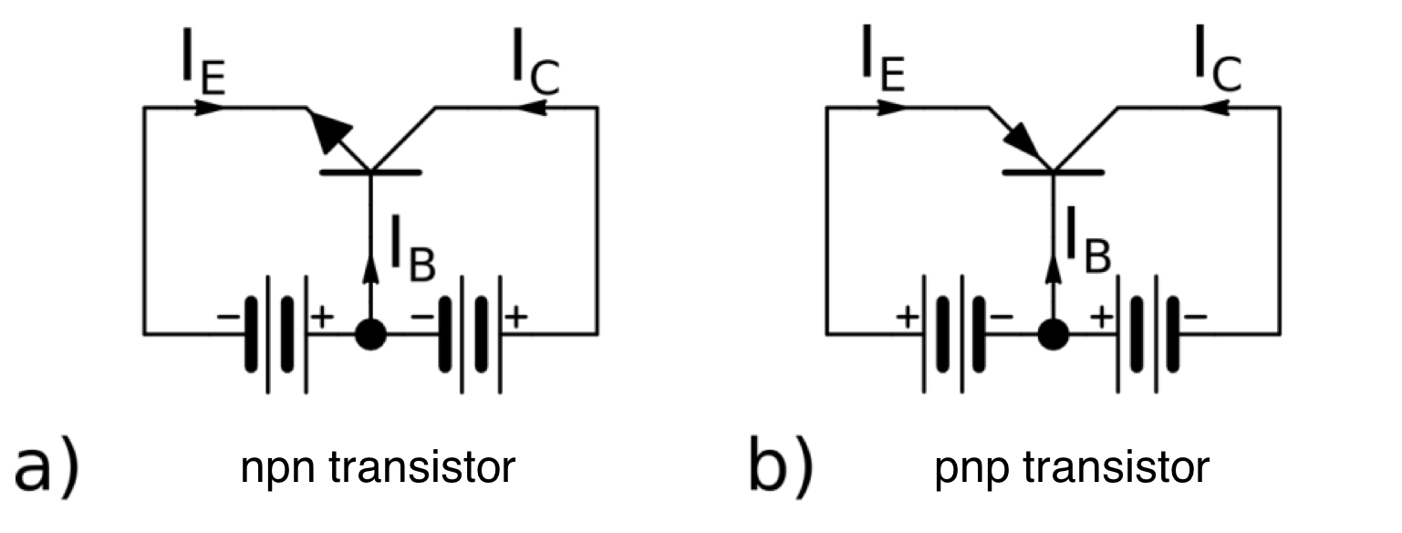
Figure 3
When discussing the operation of a transistor, the emitter current is assumed to have a finite value. When the emitter current is equal to zero, currents of thermally generated carriers flow through the backward-biased collector junction: an electron current flows from the base to the collector, and a hole current flows from the collector to the base. Together, they form a zero collector junction current \(I_{CB0}\) in a common-base system. Similarly to the saturation current of a semiconductor diode \(I_S\), the collector zero current in \(I_{CB0}\) increases with temperature (for germanium transistors almost 10 times for every 30°C increase in temperature). This dependence shifts the working point of transistors working in electronic circuits, which is unfavorable and is particularly important for germanium transistors. This property added to the reasons for replacing germanium transistors with silicon ones, which have zero collector currents several orders of magnitude (!) lower.
Ultimately, the collector current relates to the emitter current and the zero collector current as follows:
\( I_C = I_{CB0} - \alpha I_E \) (1)
Note that \(I_C = I_{CB0}\) when \(I_E = 0\), as defined by \(I_{CB0}\). Typical values for the current gain \(A \approx \alpha \) in a common-base and common-base system \(I_{CB0}\) are:
- For germanium transistors (here: pnp) \(A \approx \alpha = 0.98\) \(I_{CB0} = - 1\mu A\) at 20°C and -10 \(\mu A\) at 50°C
- For silicon transistors (here: npn) \(A \approx \alpha = 0.995\) \(I_{CB0} = 0.2nA\) at 20°C and -1.0 nA at 50°C
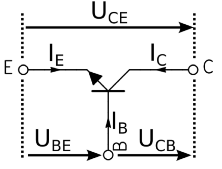
Figure 4
The figure shows that the currents \(I_E\), \(I_B\), \(I_C\) are related by the equation:
\( I_E + I_B + I_C = 0 \) (2)
Similarly, for the voltages between the terminals, the equation applies:
\( U_{CB} + U_{BE} - U_{CE} = 0 \) (3)
Thus, the given equations show that to fully describe a bipolar transistor, only two currents and two voltages need to be known, so only 4, not 6 quantities. The choice of these quantities depends on the transistor switching arrangement.