Characteristics and parameters of a bipolar transistor - theoretical introduction
Main topics:
- the principle of operation of the bipolar transistor,
- characteristic of a bipolar transistor,
- transistor transfer characteristics,
- equivalent diagram of the transistor,
- operating ranges of the transistor and limitations of its operating conditions.
Characteristic of a bipolar transistor
The operation of a bipolar transistor in static conditions, i.e. for direct current, is usually presented in the form of two families of characteristics: one for the input circuit, the other for the output circuit. These two families of characteristics unambiguously describe the static properties of the transistor. However, since it has 3 terminals, one of them is common for the input and output circuits. Therefore, the transistor can be connected to the rest of the electrical network in one of three ways; it is said that the transistor can be turned on in a common-base, common-emitter (most common) or common-collector configuration (see figure below):

Figure5: Configuration of switching on the transistor: common base (left figure), common emitter (middle figure) and common collector (right figure).
Consider a common emitter circuit with an npn transistor. The figure below shows the dependence of the base current \(I_B\) on the voltage between the base and the emitter \(U_{BE}\), where the parameter is the voltage \(U_{CE}\) between the collector and the emitter.
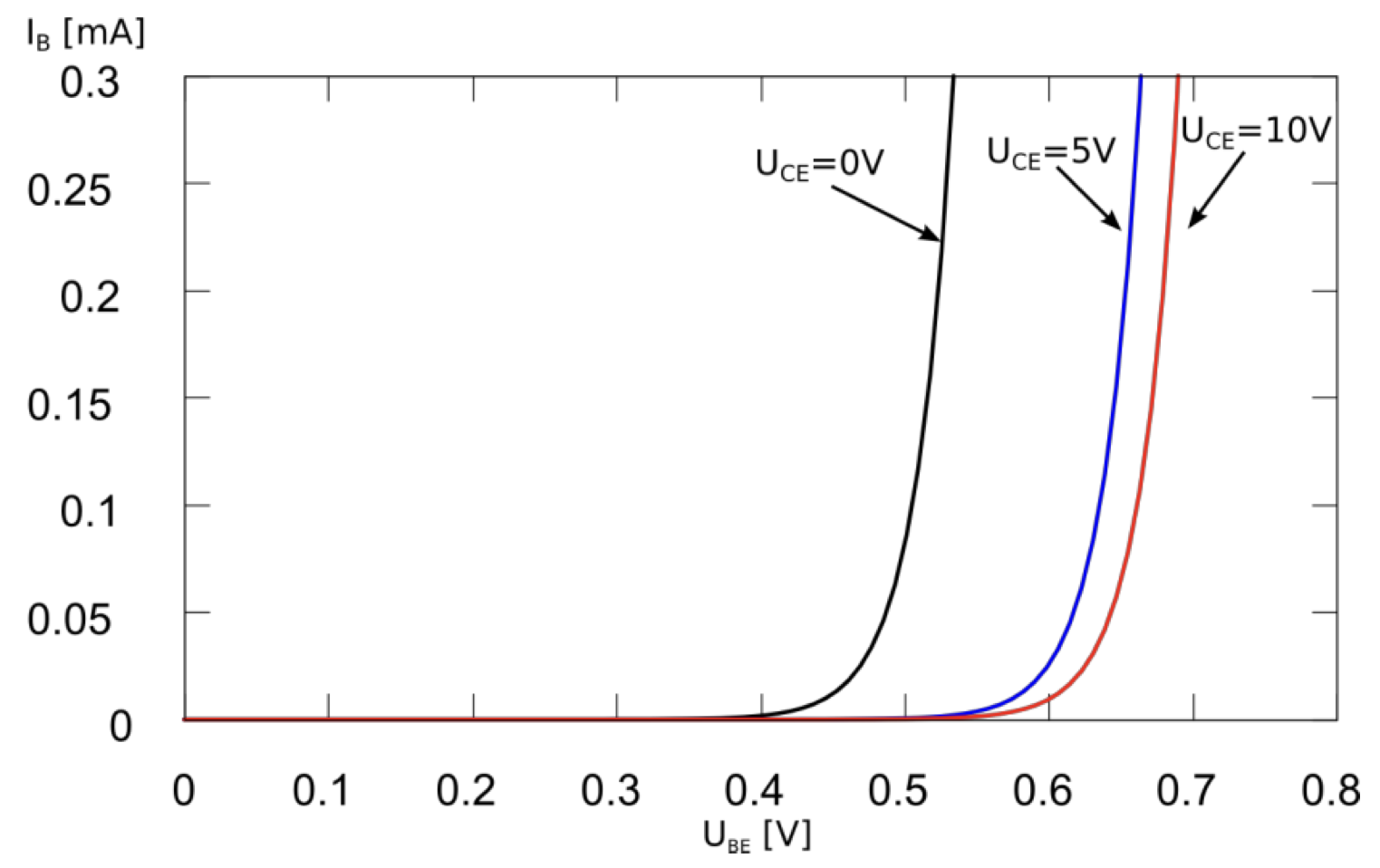
Figure6
The figure below illustrates a family of curves of dependence of the collector current \(I_C\) on the voltage between the collector and the emitter \(U_{CE}\), where the parameter of the curves is the base current \(I_B\).
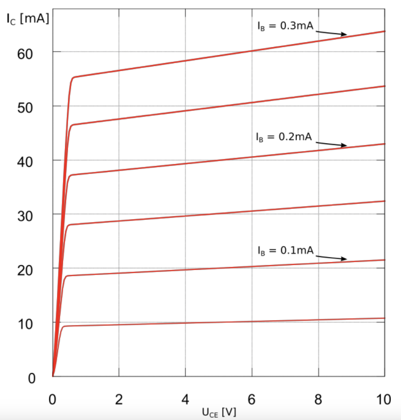
Figure7
The input characteristic of a bipolar transistor is approximately exponential and is similar to that of a diode:
\( I_B = I_{Bs} \left [ e^{\frac{U_{BE}}{U_T}} -1 \right ] \) (4)
The slight dependence of the input characteristics on the voltage \(U_{CE}\ (not included in the above equation!) is the result of the base width modulation phenomenon (the width of the current carrier depletion layer in the reverse biased collector junction).
We will discuss the output characteristics from Figure 7. The characteristic corresponding to \(I_B = 0\) lies very close to the voltage axis, although it does not coincide with it. This follows from equations (1) and (2) on the previous page, rearranged to express \(I_C\) by \(I_B\):
\( I_C = I_B \frac{A}{1-A}+I_{CB0} \frac{1}{1-A}=BI_B + I_{CE0} \) (5)
where:
\( B= \frac{A}{1-A} \) (6)
is the static current gain of the transistor in a common-emitter system, and:
\( I_{CE0} = \frac{I_{CB0}}{1-A} \) (7)
is the zero collector current in a common emitter system.
Formula (5) shows that when \(I_B = 0\), i.e. when the base circuit is open, a current \(I_{CE0}\) flows in the collector circuit, which, due to the fact that \(A\) in expression (7) is close to unity, it can take significant values.
In the linear region of characteristics, small values of the base current correspond to significant values of the collector current. This is due to the fact that the current gain \(A\) is close to unity, as a result of which the current gain \(B\) reaches significant values based on equation (6). Typical values of the current gain \(B\) in a common-emitter system and the zero current \(I_{CE0}\) are:
- For germanium transistors (here: pnp) \(B = 50\) \(I_{CE0} = -50\mu A\) for \(20^oC\) and \(-500\mu A\) for \(50^oC\).
- For silicon transistors (here: npn) \(B =200\) \(I_{CE0} = 40nA\) for \(20^oC\) and \(200nA\) for \(50^oC\).